Programmatic Layout with Kicad and Python
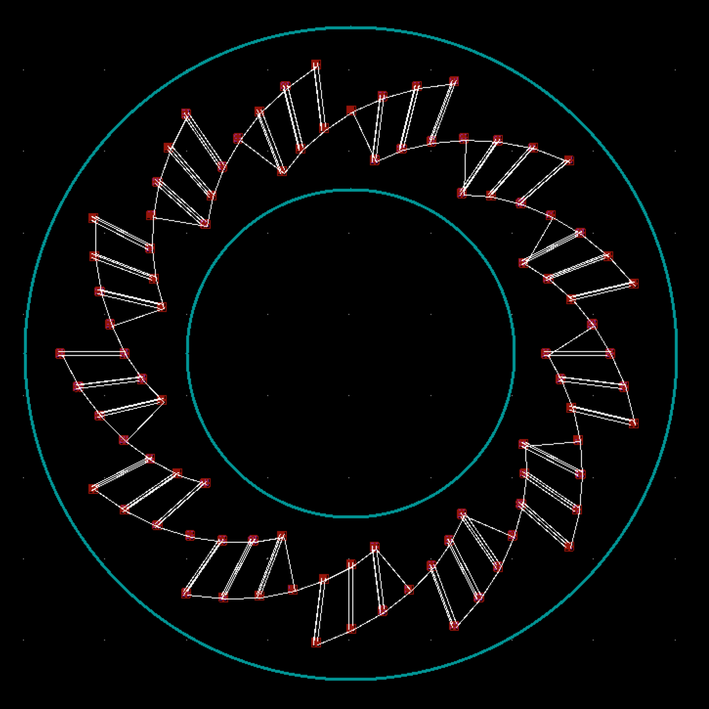
For a very geometric/repetitive design, it may be easier to describe it with code than to place parts manually. To arrange LEDs at regular spacing around a circle, I used the KiCad python API.
Update: Check out my more recent component layout plugin for a better way
KiCad has a python API that you can use to place and position footprints into a PCB design by script. The API isn't super well documented, but it turned out to support what I needed it to after a bit of research and reading the code. The biggest hurdle I had to get over was realizing that you should not modify a PCB from the python console while the design is open! The very existence of the scripting console dialog led me to believe this would be OK, but actually all of the examples are saw using this console were performing read-only operations, and making changes caused a lot of unexpected behavior.
The script below loads an existing .kicad_pcb file, adds a bunch of LED footprints, connects their pads to the appropriate nets, and then saves out to a different PCB file.
The easiest way I found to run this was to open the scripting console in pcbnew and source the
script (e.g. exec(open('generate.py').read())), because getting all of the pcbnew libraries setup
in a python env on OS X looked like a major pain.
I think you can also add tracks, and I was intending to do even some of the interconnect on these LEDs via python, but then I ended up going a different direction with this project and dropped it.
import math
import pcbnew

# All linear dimensions in mm
R1 = 1.0*25.4 # Inner diameter
R2 = 2.00*25.4 # Outer diameter
RADIAL_PITCH = 10 # Center-to-center distances radially
SEGMENTS = 52 # Number of angular segments, or "radials" to lay out
STAGGER_PERIOD = 4.0 # Number of different staggered starting radii
board = pcbnew.LoadBoard('copy.kicad_pcb')

# Converts mm to PCB internal units
SCALE = 1000000

LIBPATH = 'ColorWheel.pretty'
FOOTPRINT = 'CREE_RGBLED_1x1mm'

CENTER = (140, 95)

io = pcbnew.PCB_IO()

staggerIdx = 0.0

totalLeds = 0

def find_layer(board, layer_name):
    for i in range(128):
        if board.GetLayerName(i) == layer_name:
            return i
    return -1

def find_pad(module, padName):
    for pad in module.Pads():
        if pad.GetPadName() == padName:
            return pad
    return None

anodeNet = pcbnew.NETINFO_ITEM(board, "VLED")
board.Add(anodeNet)

# Add LEDs
for seg in range(0, SEGMENTS):
    ledCount = 0
    theta = 2*math.pi / SEGMENTS * seg
    r = R1 + RADIAL_PITCH / 2.0 + (staggerIdx / STAGGER_PERIOD)*RADIAL_PITCH
    staggerIdx = (staggerIdx + 1) % STAGGER_PERIOD
    rNet = pcbnew.NETINFO_ITEM(board, "R%02d" % seg)
    gNet = pcbnew.NETINFO_ITEM(board, "G%02d" % seg)
    bNet = pcbnew.NETINFO_ITEM(board, "B%02d" % seg)
    board.Add(rNet)
    board.Add(gNet)
    board.Add(bNet)
    while r < R2 - RADIAL_PITCH/2.0:
        newMod = io.FootprintLoad(LIBPATH, FOOTPRINT)
        newMod.SetReference("D%d-%d" % (seg, ledCount))
        x = CENTER[0] + r * math.cos(theta)
        y = CENTER[1] + r * math.sin(theta)
        newMod.SetPosition(pcbnew.wxPoint(x*SCALE, y*SCALE))

        board.Add(newMod)

        find_pad(newMod, '1').SetNetCode(rNet.GetNet())
        find_pad(newMod, '2').SetNetCode(gNet.GetNet())
        find_pad(newMod, '3').SetNetCode(bNet.GetNet())
        find_pad(newMod, '4').SetNetCode(anodeNet.GetNet())

        ledCount += 1
        totalLeds += 1
        r += RADIAL_PITCH
print("Added %d LEDs" % totalLeds)

# Add silkscreen border
silkLayerId = find_layer(board, "F.SilkS")
if(silkLayerId == -1):
    print("Couldn't find silk screen layer")

for radius in [R1, R2]:
    circle1 = pcbnew.DRAWSEGMENT()
    circle1.SetShape(pcbnew.S_CIRCLE)
    circle1.SetCenter(pcbnew.wxPoint(CENTER[0]*SCALE, CENTER[1]*SCALE))
    start_coord = pcbnew.wxPoint(CENTER[0]*SCALE, (CENTER[1] + radius)*SCALE)
    circle1.SetArcStart(start_coord)
    circle1.SetLayer(silkLayerId)
    circle1.SetWidth(int(0.5*SCALE))
    board.Add(circle1)


board.Save('autogen.kicad_pcb')